Next-Level Electronics Manufacturing with Plasma Technology
Please download press release and images here
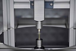
Plasmatreat GmbH, a global leader in the development and manufacturing of atmospheric pressure plasma systems and equipment, will showcase state-of-the-art solutions for particle-free, contactless, chemical-free, and inline-compatible surface pretreatment in semiconductor and electronics manufacturing at SEMICON Europa in Hall B1136 and at productronica 2025 in Hall A2, Booth 445. The focus will be on new nozzle solutions for Openair-Plasma technology and processes for flux removal and rapid oxide reduction. Potential-free plasma reliably removes organic and inorganic residues, selectively activates surfaces, and reduces oxides inline. Using plasma increases yield and process stability, improves adhesion, and enables resource-saving, VOC-free manufacturing processes.
Electronics manufacturing is under significant pressure due to miniaturization and increasing power densities. These factors require surfaces that are absolutely clean, oxide-free, and wettable, and that are reliably prepared for hybrid/chiplet bonding and wafer-level packaging. At the same time, flux residues and oxide layers must be removed without chemicals, cleanroom specifications must be met, and cycle times must be reliably achieved. Potential-free, low-particle, and dry processes that can be integrated inline are needed. These processes must be both locally precise (selective) and homogeneous over large areas. These processes result in stable interfaces, higher yields, and sustainable process chains without VOCs or aggressive media.

SEMICON Europe: Contactless Plasma Treatment for Maximum Purity in Semiconductor Manufacturing
At SEMICON Europe 2025, Plasmatreat will present cutting-edge solutions for particle-free, contactless surface treatment in semiconductor production. The focus will be on new nozzle solutions based on Openair-Plasma technology that have been specially developed for hybrid bonding, wafer-level packaging, and advanced assembly requirements.
World premiere – new nozzles specially designed for the challenges of semiconductor manufacturing
The presentation will focus on two new plasma nozzles. First is the new DBD nozzle, PDW100, which is a flat, atmospheric plasma application with a treatment width of up to 100 mm. It enables the uniform activation of large areas of sensitive substrates and removes organic residues and oxides without generating particles, ensuring high process stability.
Second, Plasmatreat will present the PFA10 plasma nozzle. It provides a low-particle, potential-free, and precise local plasma treatment. The PFA10 removes organic residues and oxide layers, activates metallic and polymer surfaces, and creates optimal conditions for hybrid bonding and chiplet stacking.
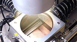
Plasmatreat uses a compact demo unit to show how wafers are precisely moved between two plasma process stations using a contactless transport system (XPlanar from Beckhoff), eliminating mechanical abrasion and particle formation. This creates an ideal environment for the contamination-free pretreatment of sensitive substrates under cleanroom conditions.
"With the expansion of our plasma nozzle range, we can take purity and process reliability in semiconductor manufacturing to a new level," explains Nico Coenen, Plasmatreat's Global Director of Electronics Markets. “The PFA10 and PDW100 enable uniform, contamination-free surface treatment, which is essential for reliable electrical and mechanical connections — even in cleanroom class 1 environments.”
Plasmatreat's Openair-Plasma Technology is dry, chemical-free, and inline-capable. It reliably removes organic contaminants, silicones, and electrostatic dust while increasing surface energy to over 72 mN/m—ideal for subsequent processes such as die bonding, wire bonding, or underfill. The treatment takes place in a matter of seconds, delivers consistent results, and uses cost-effective process gases, such as compressed air or nitrogen.

productronica: Broad and Flexible Portfolio of Solutions for Electronics Manufacturing
At productronica 2025, Plasmatreat will present its comprehensive range of Openair-Plasma solutions for electronics manufacturing, including applications for PCB assembly, coating, and the treatment of leadframes and power modules. Depending on the process step and application, Plasmatreat offers customized systems for cleaning, activation, coating, or reduction — always dry, VOC-free, and inline-capable.
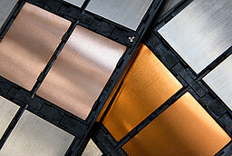
A notable highlight is the REDOX-Tool, which removes oxide layers from metal surfaces inline and in sync with production — without the use of formic acid. This process is chemical-free, reproducible, and automatable. PlasmaPlus will also be on display as a nanolayer technology that promotes adhesion for overmolding, sintering, and bonding processes. This process prevents delamination in epoxy mold compounds and achieves excellent adhesion up to MSL 1. Another trade fair highlight is HydroPlasma, which removes flux residues from the soldering process using water, compressed air, and electricity. This process is solvent-free and particle-free, forming the basis for fluxless TCB and clean PCB assemblies.
Visitors to the Plasmatreat booth can experience these applications live. Modular systems with static or rotating nozzles, generators, and plasma control units demonstrate the reliable treatment of sensitive components. Trade visitors can discuss individual solutions directly with plasma experts.
"Our portfolio of solutions covers all manufacturing steps — from front-end to back-end, lead frame treatment to PCB manufacturing, assembly, and conformal coating," says Nico Coenen. “Whether it's activation, cleaning, coating, or reduction, our plasma technologies ensure reproducible, efficient processes, improved adhesion, and greater reliability and durability.”
Plasmatreat supports manufacturers around the world as a reliable partner for process-reliable plasma solutions with its global sales and service network.

